| Page : | [ 1 ] | [ 2 ] | [ 3 ] |
Here's some pics of making the circuit board. The pics are just through the process of etching, tinning, adding solder mask, drilling and cutting. In the pics I have some of version 1 (PWM LEDs) and some of version 2 (WS8211 LEDs).
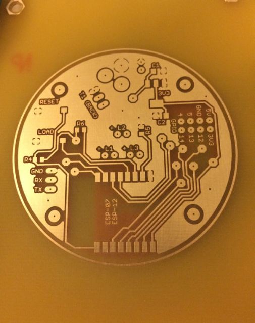
Front of V1 after etching and tinning:
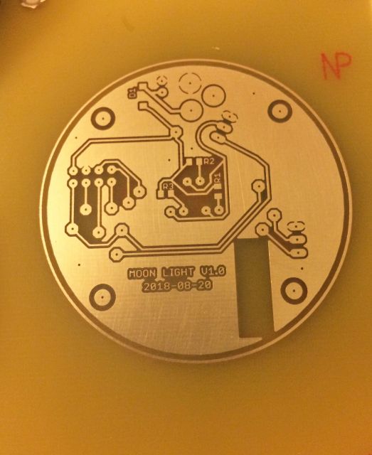
Back of V1 after etching and tinning:
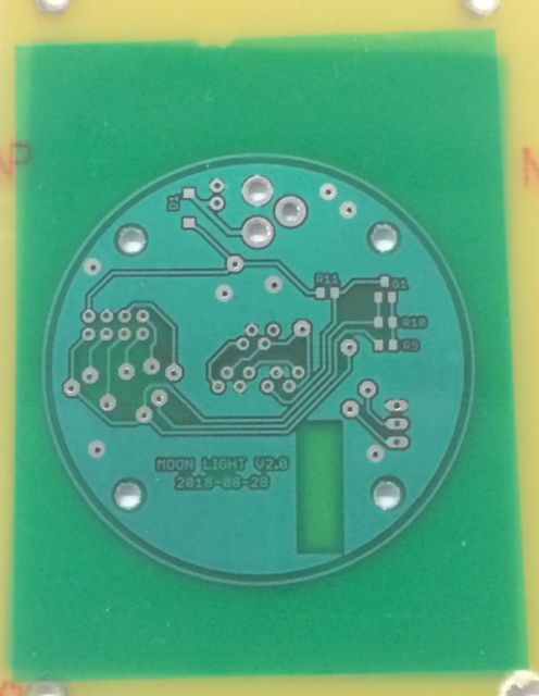
Front of V2 after applying solder mask:
Back of V2 after applying solder mask:
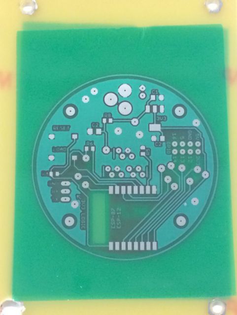
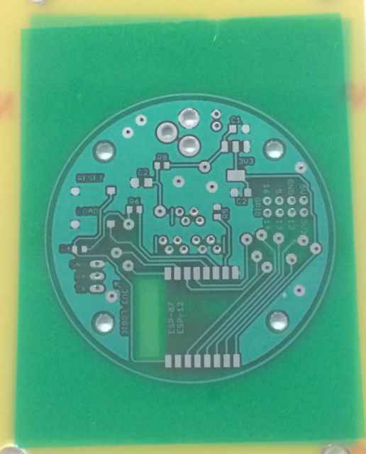
Front of V2 after drilling:
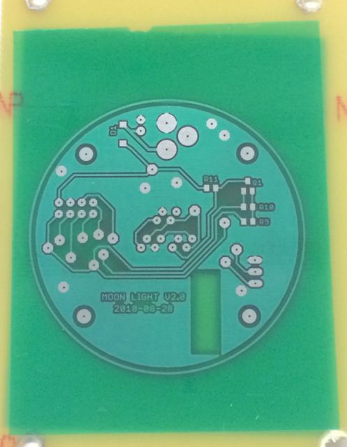
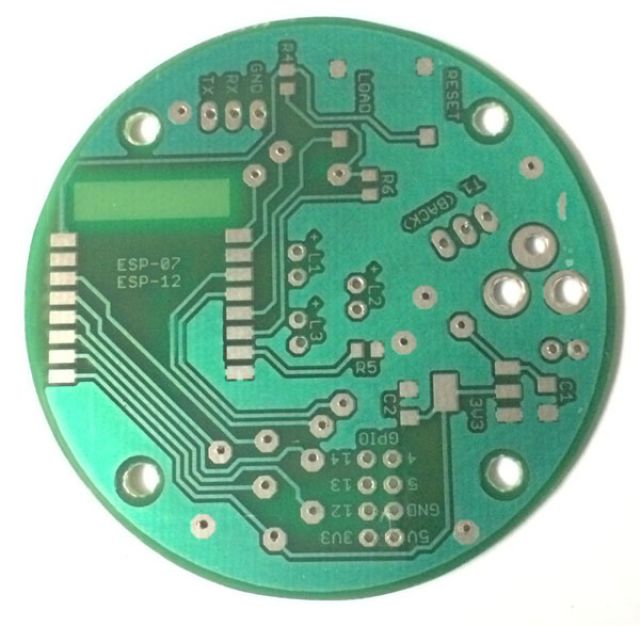
Back of V2 after drilling:
Front of V1 after cutting to shape:
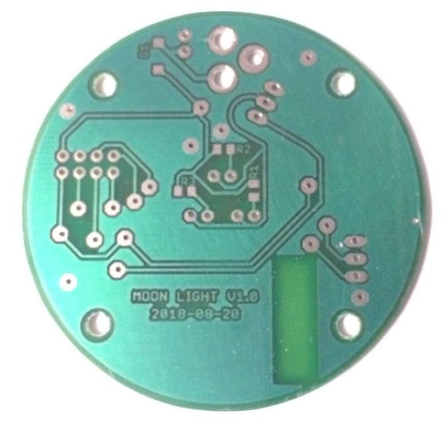
Back of V1 after cutting to shape:
| (Page 2 of 3) | ||