| Page : | [ 1 ] | [ 2 ] | [ 3 ] | [ 4 ] | [ 5 ] | [ 6 ] |
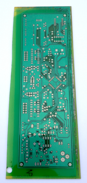
Main board after etching and solder mask:
Try to ignore the poor pictures with the reflections and shadow :)
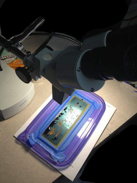
The front of the board had all sorts of problems when etching. It seems like there was some inconsistencies in the copper and/or positive resist so theres some areas where it etched all "streaky". Luckily it didn't encroach too much onto the traces. It still required some manual intervention under a microscope to see where to apply some targeted etching fluid to finish the job in those specific areas. After the solder mask was applied it still looked pretty good! I think these particular boards were of a bad batch since the positive resist was also problematic and had blemishes across many boards. I had to make do with this one since I was in danger of running out of PCB material of that length (200mm).
This side didn't have any of the problems with the copper that the other side exhibited.
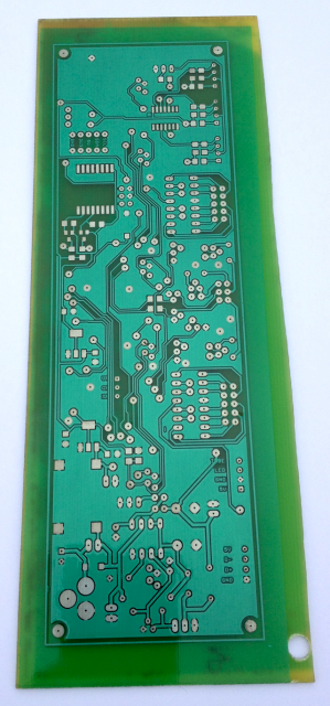
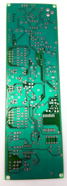
After cutting and drilling everything was good to go! :)
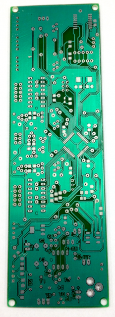
Heres a pic of the touchup work mentioned before on the side that had issues with the copper etc.
| (Page 2 of 6) | ||